Planar Conductors#
Many practical current-carrying structures, such as those found in PCBs (Printed Circuit Boards), are planar conductors—traces confined to a flat layer. These conductors are common in power electronics, RF systems, and magnetic sensors, where the geometry of the current path directly influences the magnetic field distribution and system performance.
Planar layouts are especially useful for creating compact coils, inductors, or loops within a single layer of copper. Understanding the magnetic fields generated by these structures is essential for optimizing electromagnetic behavior and minimizing interference.
In the following example, we construct a planar spiral coil using the TriangleStrip class.
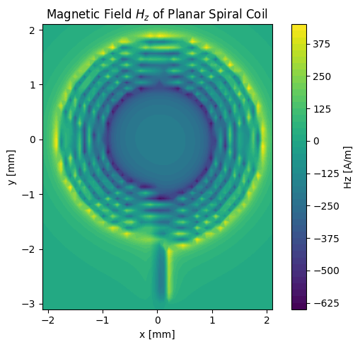
The following code computes and visualizes the z-component of the magnetic field generated by the planar coil in a plane slightly above its surface. A relatively low spatial resolution is used to reduce the computational load (~100 triangles + 2500 observers = 250000 instances), ensuring fast and lightweight execution in the documentation environment.
Note that planar coil structures are often combined with a shielding layer or a highly permeable back-sheet (e.g., ferrite) to reduce electromagnetic interference or enhance inductance. While Magpylib does not simulate induced magnetization or solve for current density distributions in materials, in such cases the Method of Images can be applied.
Keep in mind that real current distributions are typically non-uniform, especially near corners, sharp bends, or under high-frequency (AC) conditions where eddy currents become relevant. However, if the AC penetration depth is significantly larger than the conductor dimensions, eddy current effects are minimal, and the static field models provided by Magpylib can still offer reasonable approximations.